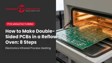
The concept is straightforward. The execution is not. Results vary significantly based on which process you choose (all solder paste versus a solder paste and adhesive hybrid), how you distribute components across sides, how your reflow profile is tuned for the second pass, and whether your oven delivers consistent heat zone-to-zone. Getting any one of these wrong can ruin a board — or a batch.
This guide covers what you need before starting, the 8 steps to execute the process, the four parameters that most influence yield, the most common failure points, and when double-sided reflow isn't the right call at all.
Key Takeaways
- Solder the lighter-component side first — it faces down during the second pass
- Run a reduced peak temperature on the second pass to avoid remelting first-side joints
- Use high-Tg FR4 (Tg ≥170°C) to reduce warping risk across two thermal cycles
- Run AOI between passes, not just after — catching defects early prevents compounding failures
- Trace most double-sided reflow failures back to setup decisions, not equipment faults
What You Need Before Making Double-Sided PCBs in a Reflow Oven
Preparation quality directly determines yield. Problems that originate here — wrong component sequencing, mismatched paste, a substrate with a low Tg rating — cannot be corrected by adjusting the oven mid-run.
Equipment and Oven Requirements
Your reflow oven needs multi-zone temperature control, programmable profiling for both passes, and stable, uniform heat distribution across the full board width. According to BTU's reflow oven selection guidance, six zones are sufficient for lab environments while eight or more are recommended for production. Repeatable profile capability matters more than hitting a specific zone count.
If you're running an infrared reflow oven, lamp condition and calibration directly affect zone-to-zone temperature consistency. IR heating responds to component color differences and thermal shadowing across mixed-density boards, so lamp quality and regular calibration are non-negotiable in production settings.
Replacement lamp quality is a practical concern here. Fannon Products manufactures short-wave, medium-wave, and fast medium-wave quartz infrared lamps — including twin-tube configurations — rated at 96% radiant efficiency with 5,000+ hour life expectancy, specifically for electronics reflow soldering applications.
Additional equipment required:
- Solder paste stencils correctly sized for both sides
- Pick-and-place tool or manual placement aids
- PCB support fixtures or carriers
- AOI or visual inspection tool
Materials and Board Readiness
Solder paste: SAC305 is standard for lead-free assemblies, with a liquidus range of 217–219°C per Kester's SAC305 technical data. For high-reliability assemblies, consider a lower-melting-point alloy such as Sn-Bi (eutectic melting point ~138°C) on the second side to allow that side to reflow at temperatures less likely to disturb first-side joints. Stencil thickness of 0.10–0.13 mm on the first side limits paste volume and reduces remelting risk during the second pass.
Board readiness checklist:
- Substrate Tg ≥170°C — Isola FR406 (Tg 170°C) and IS410 (Tg 180°C) are proven choices for double-pass reflow
- Board is clean, free of oxidation and flux residues
- Pad surfaces are coplanar
- Rail width of your oven accommodates the board dimensions
- Component layout reviewed to identify which side carries heavier parts
How to Make Double-Sided PCBs in a Reflow Oven: 8 Steps
These steps follow the all-solder-paste process, which is standard for boards with SMD components on both sides. Where the red glue hybrid process diverges, that's noted.
Step 1: Plan Your Component Layout and Choose Your Process
Identify which side carries heavier or taller components — that side becomes Side B (second pass). The lighter side becomes Side A and goes through the oven first.
- All-solder-paste process: Use when both sides carry precision ICs, BGAs, QFNs, or similar SMD components
- Red glue hybrid process: Use when one side has large connectors, electrolytic capacitors, or heavy packages that solder surface tension cannot reliably support during the second pass
Research from a SMTA/Circuit Insight study on double-sided reflow of QFNs found that weight-to-wetted-perimeter ratio is a reliable predictor of component retention during second-pass reflow — components with excessive weight relative to their solderable perimeter are fallout risks and should be flagged during this planning step.
Step 2: Clean and Inspect the PCB
- Remove contamination, flux residues, and oxidation using compressed air or an appropriate PCB cleaner
- Verify pad coplanarity
- Confirm substrate material and Tg rating
- Check board thickness — thinner boards need additional fixture support during the second pass
- Confirm your oven's rail width accommodates the board
Step 3: Apply Solder Paste to Side A
Print solder paste onto Side A pads using a correctly aligned stencil. Use a 0.10–0.13 mm stencil to apply a slightly reduced paste volume. Less solder on Side A means less material available to remelt during the second pass, reducing the risk of joint disruption.
After printing, inspect for:
- Bridging between pads
- Insufficient fill
- Misalignment
Rework before placement. Defects caught here are far easier to correct than after reflow.
Step 4: Place Components on Side A
Place all SMD components on Side A per the design layout with correct orientation. Side A should carry lighter, smaller components — passives, smaller ICs — whenever the layout allows.
Run a visual QC check or AOI scan before sending to the oven. Any misalignment is far simpler to address now than after the board has been through reflow.
Step 5: Run the First Reflow Pass (Side A)
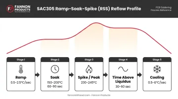
Program a standard Ramp-Soak-Spike (RSS) profile. Per Indium's Pb-free solder paste process documentation, recommended parameters for SAC305 are:
| Profile Stage | Parameter |
|---|---|
| Ramp rate | 0.5–2.5°C/second |
| Soak zone | 150–200°C for 60–90 seconds |
| Peak temperature | 230–245°C |
| Time above liquidus (TAL) | 30–60 seconds (45–60 ideal) |
| Cooling rate | 0.5–6°C/second |
Allow the board to cool fully to room temperature before flipping. Rushing the cooling phase introduces thermal stress that weakens joints.
Step 6: Flip the Board and Set Up Support for Side B
Flip the board so Side A faces down. Use PCB support fixtures, rails, or a custom carrier to prevent sagging or rocking. This is especially important for thinner boards and boards with taller Side A components now protruding downward.
Before proceeding, inspect Side A solder joints and address any of the following:
- Solder bridges between pads
- Cold or incomplete joints
- Misaligned or shifted components
The second thermal cycle will compound existing problems, not correct them.
Step 7: Apply Solder Paste and Place Components on Side B
Print solder paste onto Side B pads. This side is soldering fresh pads, so standard stencil thickness applies here. Place all Side B components with correct orientation.
Run pre-reflow AOI or visual inspection on Side B before the oven run. Confirm that heavier or oversized components are either correctly positioned for this second pass or will be hand-soldered after the oven run — don't send a component through a second thermal cycle if it exceeded the weight-to-perimeter threshold identified in Step 1.
Step 8: Run the Second Reflow Pass (Side B) and Inspect
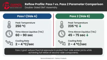
Program a modified reflow profile for Side B. Reduce the peak temperature compared to the first pass to keep first-side joints below full liquidus while the second side solders properly. SAC305 paste specifications typically target a peak of 230–245°C for standard assemblies. Targeting the lower end of that range for Pass 2 keeps Side A joints from re-liquefying while the second side solders properly.
Key profile adjustments for Pass 2:
- Reduce peak temperature from Pass 1 levels
- Maintain TAL of at least 30–45 seconds for reliable second-side joint formation
- Keep cooling rate at 0.5–4°C/second
After the second pass, allow full cool-down, then conduct thorough AOI on both sides. Check for:
- Component shift or displacement on Side A
- Solder bridges on Side B
- Cold or grainy joints on either side
- Any signs of board warping
Address defects by touch-up soldering or targeted rework before the board moves forward.
Key Parameters That Affect Double-Sided Reflow Results
Even with correct steps, four variables drive outcomes — and they interact. Poor control of any single one can produce defects across the whole board.
Peak Temperature and Differential Between Passes
If the second-pass peak is too high, first-side solder joints fully remelt and gravity pulls components off the flipped board. Too low, and the second side produces cold joints.
SAC305 has a liquidus range of 217–219°C. The second-pass peak needs to clear this threshold reliably for second-side joints while staying as far below it as practical for first-side joints. If second-side reliability is critical, switching to a lower-melting-point alloy (Sn-Bi, liquidus ~138°C) on Side B allows that side to reflow at temperatures well below SAC305's liquidus, directly protecting first-side joints.
Component Weight and Pad Coverage
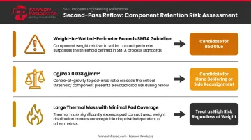
Solder surface tension can support lighter SMD components during the second pass, but it has limits. The SMTA/Circuit Insight QFN weight study established that weight-to-wetted-perimeter ratio — not just weight alone — is the better predictor of retention risk for components like QFNs.
MPE Research puts the risk threshold at Cg/Pa ≤ 0.038 g/mm² for avoiding drop-off. Use both metrics during Step 1 layout planning to flag components that need intervention:
- Weight-to-wetted-perimeter ratio exceeds SMTA guidelines → candidate for red glue
- Cg/Pa > 0.038 g/mm² → candidate for hand soldering or side reassignment
- Large thermal mass with minimal pad coverage → treat as high-risk regardless of weight
Board Support and Flatness
Without proper support, PCBs sag or warp under heat, causing component misalignment and uneven solder flow. This is worse on thin boards and larger-format panels. Support fixtures maintain flatness, distribute weight evenly, and prevent contact damage to Side A components facing downward.
For production runs, custom-fitted carriers are worth the investment. They eliminate board-to-board variation in support quality that translates directly to yield variation.
Ramp Rate and Soak Duration
A ramp rate that's too fast causes thermal shock; too slow and heat-sensitive components experience prolonged exposure. For the second pass, a controlled ramp rate and a slightly shorter soak period reduce cumulative heat stress on already-soldered Side A joints without sacrificing flux activation on Side B. The goal is minimum thermal dose for first-side joints while still meeting the process requirements for the second side.
Common Mistakes and Troubleshooting Tips
Most double-sided reflow failures trace back to avoidable setup decisions, not random oven faults.
Mistake: Soldering the heavier side first. The heavier side must always be the second pass. Reversing this sequence removes solder surface tension as a retention mechanism precisely when you need it most: during the second pass with components facing down.
Mistake: Using the same profile for both passes. Running identical profiles for both passes risks fully remelting Side A solder during the second pass. The second pass needs a deliberately adjusted profile.
When the mistakes above do occur, here's how to diagnose and recover.
Troubleshooting: Components shifting or falling off during the second pass.
- Check component sequencing from Step 1 — was the heavier side correctly assigned to the second pass?
- Reduce second-pass peak temperature
- For heavy offenders that can't be moved to Side B, apply high-temperature epoxy adhesive beneath them before the second pass
Troubleshooting: Cold or grainy joints on Side B.
- Verify solder paste condition — paste past its shelf life shows this symptom
- Confirm peak temperature clears the paste's liquidus point with adequate TAL (30–45 seconds minimum)
- Avoid overcorrecting the second-pass profile so aggressively that the second side never reaches proper reflow temperature
Alternatives to Double-Sided Reflow Oven Soldering
Double-sided reflow isn't always the right method. Component types, board design, or production scale may make other approaches more practical.
Solder Paste + Red Glue (Adhesive) Hybrid Process
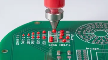
Use this when one side carries large, heavy components — connectors, electrolytic capacitors, large transformers — that exceed the surface-tension retention threshold.
Trade-offs to account for:
- Adds dispensing and curing steps to the process
- Henkel LOCTITE 3627 cures at approximately 150°C for 90–120 seconds (meaningful conversion is also achievable at 125°C)
- Dispensing accuracy must be tight enough to avoid pad contamination
- Red glue curing must always be sequenced after the solder-paste side has been reflowed, not before
Selective Soldering or Hand Soldering for Heavy Components
Best suited for low-volume prototyping, or when only a few heavy components would require red glue or create reflow complications. This approach won't scale to high-volume production — it requires skilled operators and can't match the throughput or repeatability of automated reflow for dense SMD layouts.
Wave Soldering for Through-Hole Components
The right fit when board design combines SMD on the top side (reflowed) with through-hole components on the bottom — wave soldering handles through-hole leads efficiently once top-side reflow is complete.
Keep in mind: wave soldering isn't suitable for fine-pitch SMD components on the bottom side. Top-side reflow must be fully completed first, and wave parameters need to be dialed in carefully to avoid disturbing any bottom-side SMD joints secured with red glue.
Frequently Asked Questions
Can you reflow solder both sides of a PCB without components falling off?
Yes, when lighter and smaller components are placed on the first-pass side (Side A) and the second-pass peak temperature is reduced to keep first-side joints below full liquidus during the second pass. Solder surface tension provides meaningful retention for lighter components, but the layout and profile must be planned to work within that constraint.
What is the correct reflow oven temperature for the second pass on a double-sided PCB?
The AIM SAC305 TDS specifies a peak range of 230–245°C for standard assemblies. For the second pass, target the lower end of that range — this limits remelting of first-side joints while still achieving reliable Side B soldering.
How do you prevent heavy components from falling off during second-pass reflow?
Three options: place heavy components on Side B (top side during second pass) so they face upward during reflow; apply epoxy adhesive (red glue) under components that must remain on the bottom side; or hand-solder heavy components after the oven run.
Do you need different solder paste for the first and second sides?
The same paste can technically be used for both sides. However, using a lower-melting-point alloy such as Sn-Bi on the second side is a recognized best practice for high-reliability assemblies — it allows Side B to reflow at temperatures well below SAC305's liquidus, directly reducing the risk of disturbing first-side joints.
Is an infrared reflow oven or convection reflow oven better for double-sided PCBs?
Both can handle double-sided PCBs. Convection ovens provide more uniform heat distribution across board surfaces; IR ovens deliver targeted, rapid heat but can be affected by component color variation and thermal shadowing. What matters most is multi-zone programmability and temperature consistency across passes — not oven type alone.
How do I know if my second-pass profile is damaging first-side components?
Signs include component displacement on Side A, cold or cracked joints visible under AOI or microscopy, and board warping. Before production, run a thermocouple profile with thermocouples placed on Side A pads during the second-pass run. The resulting data shows whether your profile is reaching reflow temperatures on first-side joints.